| Author: | |
| Website: | |
| Page title: | |
| URL: | |
| Published: | |
| Last revised: | |
| Accessed: |
In order for the CPU to execute program instructions, it must first load the instruction, and any operands on which it will act, into the appropriate CPU registers. A register is a small block of memory built in to the CPU that can hold a single word of data. The concept of a word is similar to that of a byte in that it holds a fixed number of bits. Whereas a byte is normally regarded as a block of eight bits, however, the number of bits in a word depends on the size of the processor's registers. In a 16-bit processor for example, a word is 16 bits long. In a 32-bit processor, it is 32 bits long, and so on. The registers in a CPU can be regarded as the fastest form of computer memory, because of the speed with which their contents can be accessed by the CPU (a few nanoseconds).
In order to get the data into the registers in the first place however, it must be fetched from wherever it is stored in the computer system. Furthermore, because of the speed at which the CPU executes program instructions (hundreds of millions per second), the instruction or data that must be stored in each register will need to change constantly and at very high speeds. Effectively, therefore, the speed at which the CPU can operate will be limited by the speed at which it can fetch instructions and data from working memory and load them into its registers prior to executing a program instruction.
If program instructions and data had to be loaded into the CPU's registers from a secondary storage medium such as a hard disk drive or CD-ROM drive, the operation of the CPU would be incredibly slow (in fact, it would not even be feasible to operate in this fashion). The programs and data are therefore loaded into a form of solid-state electronic memory (random access memory, or RAM) that is located (relatively) close to the CPU, with a dedicated data bus provided between it and the CPU.
RAM generally consists of a number of integrated circuits mounted on one or more circuit boards (memory modules) that plug into specialised slots on the mainboard. Each memory module can store hundreds, or even thousands of megabytes of data. Individual bits are stored electronically in cells, which are organised into banks. A bank consists of a number of rows (called wordlines) and columns (called bitlines). The address of a memory cell can thus be expressed using a bank number, row address, and column address.
Because each cell in memory can be addressed directly in this way, access is said to be random (as opposed to the sort of sequential access available with magnetic tape, for example, where data cannot be read until the part of the tape that actually contains the required data appears under the read-write head). One item of data in RAM can be accessed just as quickly as any other, regardless of which bank, row and column it is stored in. In addition, unlike tape drives, magnetic disk drives, or optical drives, RAM does not rely on any mechanical elements that would limit its speed of operation.
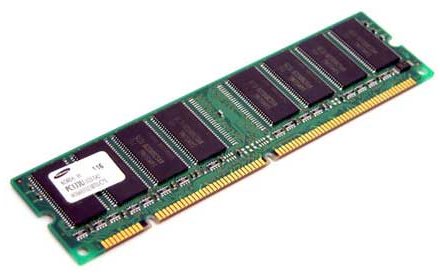
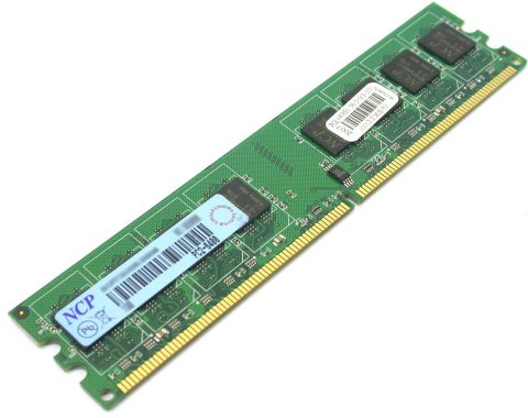
A typical memory module
Main memory is linked to the processor via the address bus and data bus. The width of the address bus determines the size of the memory space that can be addressed, while the width of the data bus (together with the size of the processor's registers) dictates how many bits of data can be retrieved from or written to memory in a single operation (or bus cycle). A 32-bit address bus, for example, will allow up to 4 Gigabytes of memory to be addressed, and enable 32 bits of data to be retrieved during each cycle. The circuitry required to support memory operations includes Row Address Select (RAS) and Column Address Select (CAS) logic.
Unlike the kind of memory used for secondary storage (magnetic disk drives, optical drives and flash drives, for example) RAM is volatile memory in the sense that, when the power is turned off, the contents of memory are lost. RAM can be further categorised as dynamic RAM (DRAM) or static RAM (SRAM). Each cell in dynamic RAM uses a combination of a transistor and a capacitor to form a memory cell that stores the state of a single bit. The transistor acts as a switch, allowing the memory control circuitry to read or write to the cell. If the capacitor is charged, the cell holds binary one, otherwise it holds binary zero.
Because of the extremely small size of the components (there are, after all, millions on a single chip), the stored charge leaks away very quickly. To prevent data loss, memory must be periodically refreshed. The refresh circuitry reads the value stored in each memory location before the charge has a chance to leak away completely, and writes the date back to memory by recharging the cells holding a binary one. The limitations on the speed of this type of memory depend on the length of the refresh cycle. Typical values are in the order of 60 - 70 nanoseconds. While the refresh process is actually taking place, the stored data cannot be accessed by the CPU.
Static RAM relies on the use of bi-stable circuits (or flip-flops). A single bi-stable circuit (which requires either two or four transistors) can be maintained in one of two states without needing to be refreshed, affording much faster access than dynamic RAM. Unfortunately, the requirement for multiple transistors means that SRAM not only occupies more space than its DRAM equivalent, but is considerably more expensive. For this reason, most commercially available computer memory currently employs DRAM in order to keep the cost of computer systems as competitive as possible.
Early types of RAM employed a parity bit to provide limited error checking. This required one additional bit to be stored with each byte of information, making so-called parity ram both more expensive and slightly slower in operation than non-parity RAM. Parity RAM is no longer used, but for critical applications (heavy-duty servers, for example) RAM is available with Extended Error Correction (EEC), in which an Error Correction Code (ECC) is added to the data to allow errors to be detected and corrected.
As with parity RAM, sufficient additional (redundant) error-checking data must be sent with the actual data in order to ensure that errors are discovered and corrected. Processing this redundant data inevitably adds to the overall time required for memory read and write operations, and the additional space required to store it adds to the cost of manufacturing memory chips. Thanks to advanced manufacturing techniques, memory modules today are extremely reliable, and most computers sold today do not require either parity or ECC memory.
Column address select latency (or CAS latency) is the interval between the time at which a memory controller tells a memory module to access a specific column in a selected row, and the time at which the data in the specified array appears on the module's output pins. In asynchronous DRAM, the interval is specified in nanoseconds. In synchronous DRAM (SDRAM), it is specified in clock cycles and must be divided by the clock frequency to convert to nanoseconds.
DRAM memory chips are made up of multiple banks internally, and data can be output from one bank during a period of CAS latency that is occurring in another. If the data to be read is known some time in advance, therefore, maximum bandwidth can be achieved and is limited only by the clock speed. If the data to be read is not predictable, however, the latency due to row and column selection will have an effect on the speed of operations.
For a completely unpredictable memory access, the latency includes the time required to select the row, plus the time required to select the column. Since many of the data words required can typically be found on the same row, the CAS latency is often the most significant factor affecting access speed. By around 2000, SDRAM had replaced most other forms of DRAM in computers.
SDRAM is synchronized with the system bus, which means that, unlike with asynchronous DRAM, incoming instructions can be pipelined. This means that a memory chip can accept a new instruction before it has finished processing the previous one. The first type of SDRAM, sometimes called Single Data Rate SDRAM (SDR SDRAM) can accept one instruction and transfer one word of data per clock cycle. Typical clock frequencies used in SDR SDRAM are 66, 100 and 133 MHz. The DRAM controller's task is a complex one, because although multiple read or write operations may be in progress at any one time, the controller must ensure that the data bus is never needed for a read and a write at the same time.
The first IBM desktop PCs used socketed dual-inline package (DIP) memory chips. This form of memory took up a lot of space on the mainboard, and was replaced towards the mid 1980s by the Single Inline Memory Module (SIMM), a small circuit board designed to accommodate multiple surface-mount memory chips. The SIMM cards were mounted in dedicated slots on the mainboard, allowing memory to be easily replaced or upgraded.
The first SIMMS were approximately 90mm long by 20mm high, and had 30 pins (or more accurately contacts), duplicated on each side of the card to provide redundancy. The 30-pin SIMM typically provided 256 kb or I Mb of memory, although 4MB and 16MB versions were produced. The 30-pin SIMM had to be installed as matching pairs (e.g. two 256 kb cards or 2 1Mb cards), and were used extensively in IBM and IBM-compatible 80286, 80386 and 80486 systems.
The second generation of SIMMs were approximately 108mm long by 25mm high (although heights could vary), and had 72 pins. By the mid 1990s, they had replaced the 30-pin version. They were deployed in 80486, Pentium, Pentium Pro, and even some Pentium II systems, and supported a 32-bit data bus. Memory sizes per card ranged from 4 Mb up to 64 Mb, and contemporary motherboards typically provided four SIMM sockets, each capable of accepting either single or double-sided SIMMS. The Pentium processor, introduced in 1993, increased the data bus size to 64 bits, which meant that the 32-bit SIMMS, if used, had to be installed in pairs. Each pair constituted a single memory bank, and was treated by the CPU as a single logical unit.
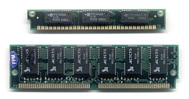
A 30-pin SIMM (top) and a 72-pin SIMM (bottom)
By 2000, memory subsystems had more or less standardised around a 64-bit data bus, and the Dual In-line Memory Module (DIMM) replaced the SIMM as the memory module standard for IBM PCs. The first SDRAM DIMMs were approximately 133mm long and 35mm high (although height could vary) and had 168 pins (84 on each side of the card). DIMMs are commonly found in Pentium and Athlon systems, and are capable of retrieving 2 x 32-bit data words (64 bits of data) in a single operation.
Unlike SIMMs, DIMMs do not usually need to be installed in pairs, and modern desktop computers typically provide only two DIMM slots. Notches in the bottom edge of the DIMM are designed to mate with lugs in the DIMM slot to ensure that the DIMM is installed with the correct orientation. SDRAM DIMMS were originally available with a bus speed of 66 MHz (PC66), and later 100 MHz (PC100) and 133 MHz (PC133). The 100 MHz and 133 MHz DIMMS could be used together on mainboards designed to operate at 100 MHz, although the 133 MHz DIMM would obviously be restricted to 100 MHz operation. As of 2007, 168 pin DIMMS are no longer used in new PCs.
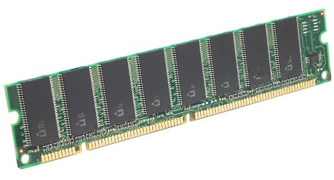
A 168-pin SDRAM DIMM
DDR SDRAM memory modules were introduced in 2002. These 184-pin DIMMs have 92 pins on each side of the card, a single notch on the bottom edge of the card, and are approximately 133mm long and 25mm high (though height can vary). They can be used either singly or in combination with other 184-pin DIMMs that operate at the same speed. The nomenclature for DDR SDRAM DIMMs reflects the maximum per-second data rate they are capable of achieving. A PC1600 memory module, for example, can deliver up to 1600 Megabits per second.
The fastest widely used form of DDR SDRAM memory module is the PC3200 DIMM, which can deliver up to 3200 Mbps. Like single data rate SDRAM, DDR SDRAM employs a 64-bit data bus. The difference is that DDR SDRAM doubles the bandwidth by double-pumping (transferring data on both the rising and the falling edge of the clock signal, without increasing the clock frequency. Data rate (in megabytes per second) is calculated as:
memory bus clock rate (MHz) × 2 × 64 / 8
Typical clock speeds are 100, 133, 166 and 200 MHz. Chips are described as DDR-200, DDR-266, DDR-333 and DDR-400 respectively, while the corresponding modules are designated as PC1600, PC2100, PC2700 and PC3200.
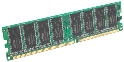
A 184-pin DDR SDRAM DIMM
DDR2 memory modules were introduced in 2003. They take the form of a 240-pin DIMM, with 120 pins on each side of the card, a single notch on the bottom edge of the card, and are approximately 133mm long and 30mm high (though height can vary). They can be used singly or in combination with other DDR2 DIMMs, and different speeds can be mixed providing the motherboard supports the fastest speed used (although the lowest speed will be used for all data transfer operations). DDR2 DIMMs can, in theory, run faster that DDR DIMMs while consuming less power.
The nomenclature for DDR2 SDRAM DIMMs reflects the maximum per-second data rate they are capable of achieving. A PC2-3200 memory module, for example, can deliver up to 3200 Megabits per second. DDR2 doubles the minimum read or write unit of DDR to 4 data words, allowing the bus rate of the SDRAM to be doubled without increasing its internal clock rate. Like DDR SDRAM, DDR2 transfers data on both the rising and the falling edge of the clock signal. The trade off is that internal operations are carried out at only half the clock rate. Where DDR-400 has an internal clock rate of 200 MHz, DDR2-400 has an internal clock rate of 100 MHz. Data rate (in megabytes per second) is calculated as:
memory bus clock rate (MHz) × 2 × 0.5 x 128 / 8
Typical clock speeds are 200, 266, 333 and 400 MHz. Chips are described as DDR2-400, DDR2-533, DDR2-667 and DDR2-800 respectively, while the corresponding modules are designated as PC2-3200, PC2-4200, PC2-5300 and PC2-6400. Be aware that DDR2 memory operated at the same external data bus clock rate as DDR memory will provide the same bandwidth but significantly higher latency, resulting in inferior performance.
By the same token, DDR2 memory operated at twice the external data bus clock rate as DDR memory will provide twice the bandwidth with the same latency. Another down side to DDR2 is the necessity of packaging them in more expensive and difficult to assemble ball grid array (BGA) packages as opposed to the thin-shrink small outline packages (TSSOPs) used for DDR DIMMs. This was necessary to maintain signal integrity at higher bandwidths.
A 240-pin DDR2 SDRAM DIMM
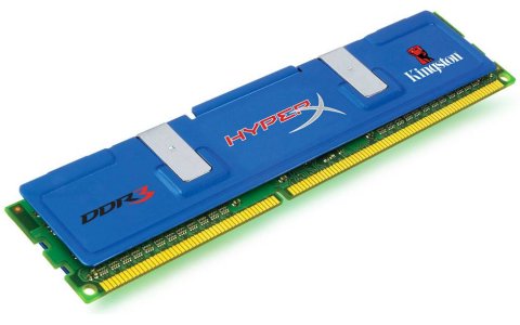
DDR3 memory modules were introduced in 2007. Like DDR2, they take the form of a 240-pin DIMM, with 120 pins on each side of the card, a single notch on the bottom edge of the card, and are approximately 133mm long and 30mm high (though height can vary). DDR3 DIMMs are faster that DDR2 DIMMs while consuming even less power.
The nomenclature for DDR3 SDRAM DIMMs reflects the maximum per-second data rate they are capable of achieving. A PC3-8500 memory module, for example, can deliver up to 8500 Megabits per second. DDR3 doubles the minimum read or write unit of DDR2 to 8 data words, allowing the bus rate of the SDRAM to be doubled without increasing its internal clock rate. Like DDR2 SDRAM, DDR3 transfers data on both the rising and the falling edge of the clock signal, although internal operations are limited to only a quarter of the clock rate. Data rate (in megabytes per second) is calculated as:
memory bus clock rate (MHz) × 2 × 0.25 x 256 / 8
Typical clock speeds are 400, 533, 667 and 800 MHz. Chips are described as DDR3-800, DDR3-1066, DDR3-1333 and DDR3-1600 respectively, while the corresponding modules are designated as PC3-6400, PC3-8400, PC3-10600 and PC3-12800.
A 240-pin DDR3 SDRAM DIMM
Systems that are capable of dual channel memory mode must have two memory modules that are exactly the same in order to utilise the dual channel facility. Dual-channel mode is implemented entirely on the mainboard, and theoretically doubles the bandwidth available for memory transfer by employing a memory controller capable of handling dual-channel operation, and two 64-bit data channels between RAM and the CPU instead of one.
Having two channels enables the bandwidth of two memory modules to be combined. One memory controller reads and writes data while the second prepares the next memory access, eliminating any setup and reset delay. It is thought that, in real terms, the increase in bandwidth over single channel architecture is in the order of 10%. Most systems that support dual channel architecture can be configured as either dual or single channel mode.
In order to utilise dual channel mode, matching pairs of DDR, DDR2 or DDR3 SDRAM DIMMs should be installed. If the motherboard has two pairs of DIMM sockets, they are often colour-coded to indicate which bank they belong to. It is theoretically possible to use paired DIMMs with different capacities in each bank, provided they can operate at the same speed.
Cache memory is a small area of static RAM (SRAM), either built into the CPU itself or located on the mainboard very adjacent to it, which is used to store frequently used program instructions and data. The basic idea is that the code or data in cache memory can be accessed far more quickly that code or data in the computer's main memory, significantly speeding up CPU operation by eliminating the delay involved in fetching instructions and data from RAM wherever possible.
Cache memory that is actually built into the CPU is called level 1 cache (or primary cache). The access time for level 1 cache is very fast. The down side is that, because it forms part of the CPU itself, its size is limited, although the size of the on-board cache (as it is called) has increased dramatically in recent years, from a few kilobytes to several megabytes.
Level 2 cache (or secondary cache) is also implemented using SRAM, but is normally located on a separate chip on the mainboard. Level 2 cache generally has far more capacity than Level 1 cache because it is external to the CPU and thus not subject to the same size constraints, but access to the contents is slower for the same reason.
When the processor needs to read from or write to memory, it first checks whether a copy of the data is in the cache. If so, the processor reads from or writes to the cache. Most modern desktop and server CPUs have at least three independent caches, including an instruction cache, a data cache, and a translation lookaside buffer (used to speed up virtual-to-physical address translation for both executable instructions and data).
If the required code or data is found in the cache, it is called a hit, otherwise it is called a miss. The hit rate is a measure of how effective the cache is. An instruction or data item not found in cache is subsequently written to cache at the same time it is retrieved from main memory, if necessary (i.e. because the cache is already full) replacing (or evicting) another code or data item (usually the least recently used).
Data written to the cache must at some point also be written to main memory. In some schemes, each write to cache is accompanied by a write to main memory. In other schemes, the cache keeps track of memory locations that have been overwritten, and only writes them to main memory when the instruction or data item stored in one of these locations is evicted from the cache.
Even in schemes where instructions or data are written to cache and memory at the same time, a number of writes to memory may be held temporarily in an intermediate storage location and periodically written to memory, to reduce the number of individual data transfer operations and improve bus utilisation. Cache coherence protocols are also implemented to ensure consistency between data in cache and data in main memory.