| Author: | |
| Website: | |
| Page title: | |
| URL: | |
| Published: | |
| Last revised: | |
| Accessed: |
A diode is an electronic component with two terminals that conducts electricity in one direction only. The term is normally used to refer to a semiconductor diode. Indeed, diodes were the first electronic components to be constructed using semiconductor materials (nowadays the material used is primarily silicon, although germanium is also used for some applications). The direction in which the diode allows current to flow is known as the diode's forward direction. In the other direction (known as the diode's reverse direction), the diode prevents current from flowing. The semiconductor material in a diode consists of two adjoining regions, each of which has been "doped" with chemical impurities to give it specific electrical characteristics.
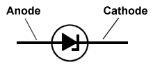
One of the regions contains a high number of negative charge carriers (free electrons) and is referred to as an n-type semiconductor material. The other region is characterised by an absence of electrons (often referred to as "holes") in many of the chemical bonds between the atoms within the region. These holes act as positive charge carriers, and the region is referred to as a p-type semiconductor material. One terminal of the diode, known as the cathode, is connected to the n-type region. The other terminal, known as the anode, is connected to the p-type region. Electrons flow from the cathode to the anode. Conventional current flow is of course in the opposite direction, so conventional current flows out of the diode via the cathode. The very nature of the diode means that it must be connected the right way round in a circuit. For this reason, most discrete diode components are marked in such a way as to identify the cathode (usually with a black or white painted band). A typical diode together with its circuit diagram symbol is shown below. Note that the direction of the arrow in the circuit symbol indicates the direction of conventional current flow through the diode.
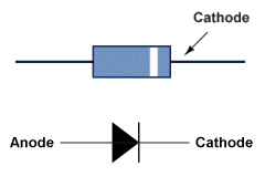
A typical diode and its circuit diagram symbol
In the two circuits shown below, a typical diode is placed in series with a lamp and a battery. In the left-hand version, the positive terminal of the battery is connected to the diode's anode so that conventional current will flow in the direction of the arrow symbol (i.e. from the anode to the cathode). The properties of the diode mean that it will permit current to flow in this direction, and the lamp will be illuminated. In the right-hand version, the battery is connected the other way round, i.e. with its negative terminal connected to the diode's anode. The diode will not conduct current in this direction, so no current flows in the circuit and the lamp remains unlit.
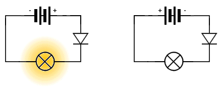
A diode will only allow current to flow in one direction
To help you to understand how a diode works, we will attempt an explanation of the properties of semiconductor materials, starting with a look at the nature of the bonds formed between the atoms that make up various materials. The first thing to understand is that for each element in the periodic table, there will be a number of electrons in orbit around the nucleus of the atom. The number of electrons orbiting the atom will be different for each element, but in all cases the atoms will be arranged in one or more orbits known as shells. Each shell requires a specific number of electrons in order to be considered complete, and the electrons in the outermost shell of an atom are known as valence electrons. It is these valence electrons that give the atom its electrical properties, which will in turn determine how the atom can combine with other atoms. The valence electrons form covalent bonds with the valence electrons of other atoms. In solids, the atoms usually combine together in a regularly repeating three-dimensional structure known as a crystal lattice. Semiconductor materials such as silicon or Germanium have four valence electrons. The structure of a silicon atom is illustrated below.
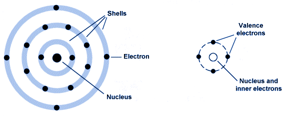
A model of a silicon atom (left) and in simplified form (right)
The outer shell of the silicon atom has four electrons. In order for the shell to be full (and thus stable), the outer shell would require eight electrons. Within the crystal lattice structure of silicon, each valence electron is shared with a nearby silicon atom to form four covalent bonds as illustrated below. Every atom thus has a 'half-share' in eight valence electrons. This number of valence electrons gives the crystal lattice a very stable structure, and also makes it very difficult for electrons to escape from their atoms. As a result, semiconductor elements such as silicon and germanium are very good insulators when in their pure state. The crystal lattice structure of a pure semiconductor material is illustrated below.
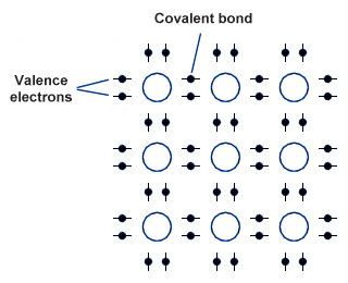
Covalent bonds in a crystal lattice
At normal temperatures, the atoms within the crystal lattice will vibrate, causing some of the covalent bonds to break and freeing valence electrons. When an electron breaks free of its bond in this way, a region of positive charge (called a hole) is created in the outer shell of the atom from whence it came, as illustrated below. The atom becomes a positive ion. The hole can be thought of as a positive charge equal in magnitude to the negative charge on an electron. Free electrons within the semiconductor material will be attracted to holes because of their opposite (positive) charge, and if an electron drops into a hole and fills it the ion becomes a neutral atom again.
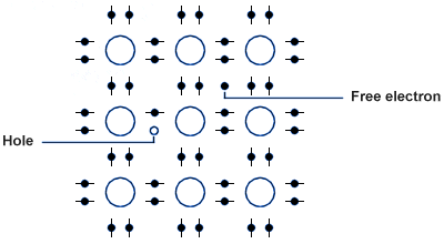
Silicon crystal lattice with free electron and hole
When a battery is connected across a pure semiconductor material, it attracts free electrons within the crystal structure to the positive terminal and supplies more free electrons at the negative terminal. The free electrons from broken covalent bonds move through the semiconductor by 'hopping' from one hole to the next towards the positive terminal, making it appear as if the positively charged holes are moving towards the negative terminal. The current that flows in a pure semiconductor material is very small, and can be thought of as streams of free electrons and holes going in opposite directions as illustrated below. This current flow is called intrinsic conduction, because the charge carriers (free electrons and holes) come from inside the material itself. The degree to which conduction occurs is also temperature dependent, since the covalent bonds break more easily as the temperature increases, creating more free electrons and holes and reducing the resistance of the semiconductor material.
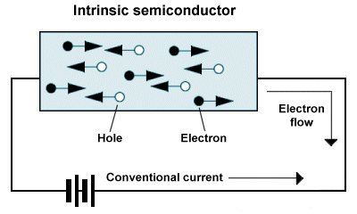
Current flow in an intrinsic semiconductor
The use of semiconductor materials to create devices such as diodes requires that the conductivity of the material be increased. This can be achieved by adding impurities to the semiconductor in a controlled way - a process known as doping. The doped semiconductor material is known as an extrinsic semiconductor because the impurities added to it introduce additional charge carriers. The materials used in the doping process must be carefully chosen. They need to have atoms of roughly the same size as the silicon or germanium atoms they are replacing, in order to be able to fit into the crystal lattice. They must also have the correct number of valence electrons to achieve the desired outcome, which is to increase the number of either negative charge carries (electrons) or positive charge carriers (holes).
In order to create a semiconductor that has a large number of negative charge carriers (known as an n-type semiconductor), the pure semiconductor material is doped with a material such as phosphorus, which has five valence electrons (and is thus said to be pentavalent). The diagram below shows what happens when a phosphorous atom is introduced into the lattice of a silicon crystal. Four of its valence electrons form covalent bonds with four neighbouring silicon atoms, but the fifth valence electron is unable to form a bond and is thus not tightly bound to the molecular structure of the crystal lattice. This "spare" electron is able to move relatively easily within the crystalline structure, and is therefore available for conduction. The impurity atom is called a donor atom because it provides an electron for conduction.
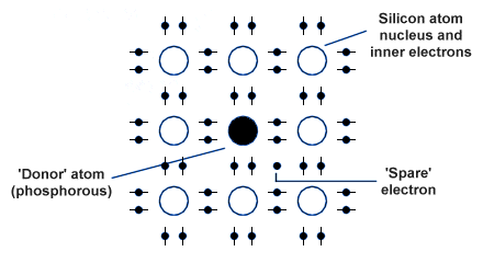
The crystal lattice structure of n-type silicon
The "impure" silicon is an n-type semiconductor since the majority charge carriers are negatively charged electrons (note that the overall charge in the crystal remains zero, because every atom in the structure remains electrically neutral). The right number of impurity atoms is added to the silicon (or germanium) to produce the required increase in conductivity. A few positively charged holes will remain in the n-type material, and act as intrinsic charge carriers. These holes are formed when covalent bonds between silicon atoms are broken. Because of the relatively small number of holes present by comparison with the number of free electrons in the material, they are called minority carriers. The diagram below illustrates conduction in an n-type semiconductor.
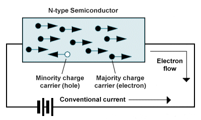
The majority charge carriers in an n-type material are electrons
In order to create a semiconductor material in which the majority charge carriers are positively charged holes (known as a p-type semiconductor), the silicon or germanium is doped using a material such as boron that has three valence electrons (and is thus said to be trivalent). The diagram below shows what happens when a boron atom is introduced into the lattice of a silicon crystal. Its three valence electrons form covalent bonds with three of the neighbouring silicon atoms. The bond between the boron atom and the fourth silicon atom remains incomplete, with the hole acting as a positive charge that can capture a free electron moving through the crystal lattice. The impurity atom is called an acceptor atom, because it will readily accept an electron in order to complete its bond with the silicon atom.
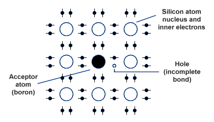
The crystal lattice structure of p-type silicon
The "impure" silicon is a p-type semiconductor since the majority charge carriers are positively charged holes (note that, as with the n-type material, the overall charge in the crystal remains zero because every atom in the structure remains electrically neutral). The right number of impurity atoms is added to the silicon (or germanium) to produce the required increase in conductivity. A few negatively charged electrons will remain in the p-type material, and act as intrinsic charge carriers. These electrons are freed when covalent bonds between silicon atoms are broken. Because of the relatively small number of electrons present by comparison with the number of holes in the material, it is electrons that now become the minority carriers. Note that for both n-type and p-type semiconductor materials, a rise in temperature will increase the number of minority carriers present in the material because the covalent bonds between the silicon (or germanium) atoms are more easily broken. The diagram below illustrates conduction in a p-type semiconductor.
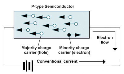
The majority charge carriers in a p-type material are holes
The operation of many semiconductor devices, including diodes, is dependent upon effects that occur at the junction between n-type and p-type semiconductor materials (the p-n junction). Such a junction, which may be formed within the same continuous crystal lattice structure using appropriate doping techniques, is illustrated below. Once the junction has been created, free electrons in the n-type material close to the junction can move across the junction (by a process known as diffusion) into the p-type material, where they occupy holes. As a result of this diffusion process, the n-type region close to the junction becomes positively charged due to losing electrons, while the p-type region on the other side of the junction becomes negatively charged due to gaining electrons. At the same time, holes appear to diffuse across the junction in the opposite direction (in fact they are created in the n-type region as a result of electrons migrating to the p-type region) and these holes may capture any remaining free electrons within close proximity.
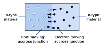
Electrons and holes close to the junction migrate across it
The movement of negative and positive charge carriers across the junction stops fairly quickly, because the increase in the negative charge in the p-type material opposes the further flow of electrons into the p-type region, while the build-up of positive charge in the n-type material opposes the creation of more holes in the n-type region. The n-type and p-type regions immediately adjacent to the junction become relatively free of majority charge carriers (see below) and together form a new region called the depletion layer. The depletion layer, although less than 10-3 mm wide, effectively becomes an insulator. A small potential difference exists across the junction, called the junction voltage, which acts from n-type to p-type. The junction voltage is about 0.1 V for germanium and 0.6 V for silicon.
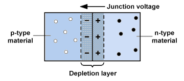
A depletion layer is created by the migration of charge carriers
If a battery is connected across a p-n junction with its positive terminal connected to the p-type side and its negative terminal to the n-type side, the junction voltage will be increased as free electrons and holes are pulled away from the junction, and the junction's resistance will become even greater. The junction is said to be reverse-biased. Electrons and holes will be repelled more strongly by the p-n junction, and the depletion layer will become wider (see below). Only a very small number of electrons and holes (created by covalent bonds breaking on both sides of the junction at normal temperatures) will be exchanged across the p-n junction, causing a tiny current (known as the leakage current) to flow.
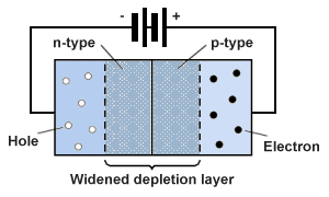
The junction shown here is reverse-biased
If a battery is connected across a p-n junction with the opposite polarity, i.e. with its positive terminal connected to the n-type side and its negative terminal to the p-type side, the junction is said to be forward-biased. The depletion layer will become narrower as free electrons and holes are pushed towards the junction, and if the applied voltage exceeds the junction voltage, current will flow across the junction because majority carriers will be able to cross it. Electrons will migrate from the n-type side to the p-type side, and holes will migrate in the opposite direction (see below). Once again there will be a leakage current due to the exchange of minority carriers created by the normal breakdown of covalent bonds on either side of the junction. This time, however, the leakage current contributes to the majority carrier current flow, and the resistance of the junction is very low.
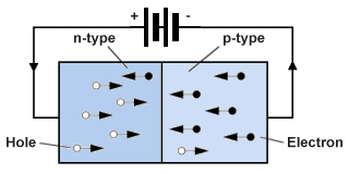
Forward bias
The junction diode is a commonly used type of diode that utilises the properties of the p-n junction. It consists of a p-n junction with one terminal connected to the p-side (the anode) and another to the n-side (the cathode). A simplified view of a silicon diode with 'planar-type' construction is shown below. A thin slice of n-type silicon is soldered to a metal base, which is connected to the cathode. A thin silicon-oxide film is formed on the upper surface of the slice by heating it in steam at about 1,100 °C, and acts as an insulating material. A 'window' is then etched chemically in the oxide film, and vapour containing the appropriate doping agent is allowed to diffuse through it, converting the exposed area of the slice into p-type silicon. Aluminium is then evaporated onto the p-type region to allow the anode lead to be soldered to it. Finally, the diode is sealed within an external casing to protect it from moisture and light.
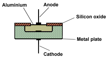
Section through a silicon diode
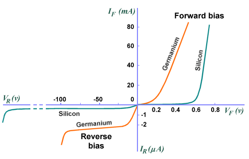
Diodes exhibit certain behaviours that make them very useful in electronic applications. When a diode is reverse-biased, it will allow only a very small leakage current to flow in the reverse direction even when the reverse voltage is relatively high. Because the diode allows current to flow in only one direction, it is a vital component in circuits that convert alternating current to direct current (a process known as rectification). Another interesting characteristic of the diode is that when forward biased, its forward voltage does not increase significantly even when relatively high currents are flowing through the diode. Typical characteristic curves for silicon and germanium diodes at 25 °C are shown below. Note that for both types the forward current (I F) is small until the forward voltage (VF) is about 0.6 V for silicon and about 0.1 V for germanium. Thereafter, a small change in VF causes a large increase in I F.
Characteristic curves for silicon and germanium diodes
The reverse current I R is negligible, and remains so as the reverse voltage VR is increased. If VR is increased sufficiently, however, the insulation of the depletion layer breaks down and I R increases suddenly and rapidly. If this occurs, the result is usually permanent damage to the diode. The breakdown voltage can vary from a few volts up to 1,000 volts for silicon and 100 volts for germanium, depending on the construction of the diode and the degree of doping used (thanks to my friend Klaus Pohlmann for pointing out that my original diagram did not show a breakdown point for the silicon curve!). Two important electrical properties of a diode are the average forward current and the maximum reverse voltage, which should not be exceeded under normal conditions.
Electricity is generated as alternating current because this is the most economical form in which to generate and distribute high volumes of electrical power. The electricity coming into your home (if you live in the UK) is 230 V alternating current with a frequency of 50 Hz. Many electronic devices, however, require relatively low voltage direct current for their operation. Diodes can be used to create circuits that rectify an alternating current in order to produce direct current. Alternating current is so-called because current flows first in one direction, and then in the opposite direction. This change of direction occurs many times per second, depending on the frequency of the a.c. supply. The simplest kind of rectifier circuit is called a half-wave rectifier, and only allows one half of the a.c. waveform to pass through a circuit. The half-wave rectifier employs a single diode which conducts electricity when the current is flowing in one direction, but not when it is flowing in the other direction. A basic circuit for a half-wave rectifier is shown below.
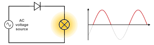
A basic half-wave rectifier
In the circuit shown, the rectified current is effectively illuminating a lamp by pulsing it with one half-cycle of the alternating current for each full cycle that occurs (only half of the a.c. waveform is allowed to pass through the diode). If the diode were to be removed, the lamp would receive current during both half-cycles and would consequently burn more brightly. Although the light burns relatively dimly, it does not blink on and off, because the filament does not have time to cool down and heat up again between half-cycles. For most applications, however, both half-cycles of the a.c. waveform will be required, and the simple half-wave rectification provided by a single diode will not suffice. A conversion circuit that makes both half-cycles of an a.c. supply available as direct current is called a full-wave rectifier. One of the most commonly used full-wave rectifier circuit designs makes use of four diodes in an arrangement called a full-wave bridge. The circuit is shown below.
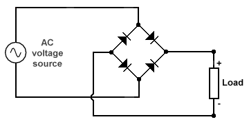
A full-wave bridge rectifier
The two circuit diagrams below show how conventional current flows in the circuit and through the load for each half-cycle of the a.c. waveform. In each case, the current flowing towards the load from the a.c. source is shown using red arrows, while the return current (from the load back to the source) is shown using blue arrows. Note that, regardless of the polarity of the half-cycle, the current always flows in the same direction through the load. In each half cycle, a different pair of diodes will be forward-biased, and will allow current to pass in the forward direction (the diodes shown in grey for each half-cycle are reverse-biased, and will block current flow in the reverse direction).
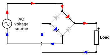
Conventional current flow in the positive half-cycle
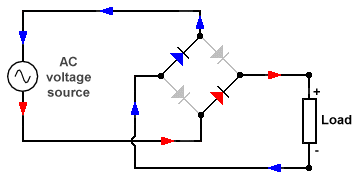
Conventional current flow in the negative half-cycle
The construction of a germanium point-contact diode is shown below. The tip of a gold or tungsten wire presses on a pellet of n-type germanium. During manufacture, a brief current is passed through the diode and produces a tiny p-type region in the pellet around the tip, forming a p-n junction with a very small area.
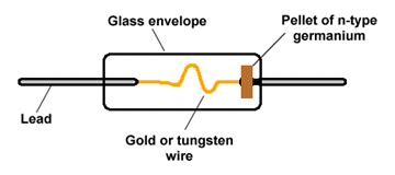
Construction of a point-contact diode
When reverse-biased, the depletion layer in a diode acts as an insulator sandwiched between two conducting 'plates' (the p-type and n-type regions). As a result, the diode acts as a capacitor. The subject of capacitors is dealt with elsewhere, but essentially a capacitor is a device that can store electrical charge. Capacitors also have the property of blocking direct current while allowing alternating current to flow, especially at high frequencies such as those found in radio signals (the higher the a.c. frequency, the less the capacitor opposes the flow of current). Point-contact diodes (sometimes called crystals) are often used as signal diodes to detect radio signals.
The point-contact diode is often used for high frequency signal detection because of its tiny junction area and hence small capacitance, which makes it sensitive to the kind of low-power, high frequency currents found in radio signals. Germanium point-contact diodes are commonly used as detectors in radio circuits because of their relatively low forward voltage (about 0.2 V), which allows them to detect lower signal voltages. Radio signals essentially consist of audio frequency signals modulated onto a radio frequency carrier. The detector works by effectively acting as a half-wave rectifier, turning the alternating current radio signal into an oscillating direct current signal. This signal is then sent through a low-pass filter to retrieve the original audio frequency signal.
In a normal junction diode, operating the diode at or above its breakdown voltage will cause the depletion layer to breaks down and result in permanent damage to the diode. Zener diodes are diodes that can be made to conduct current in the reverse direction at a specific fixed reference voltage (their breakdown voltage) without suffering damage. Each Zener diode is designed to have a specific reverse breakdown voltage (from 2.4 V upwards) at which it will conduct current in the reverse direction, and has a maximum power rating (typical values are 400 mW and 1.3 W). A Zener diode can be used on its own to provide a voltage-sensitive switch, or in series with a current-limiting resistor to provide voltage regulation. The circuit diagram symbol for a Zener diode is shown below, together with the characteristic curve for a typical Zener diode.
The circuit diagram symbol for a Zener diode
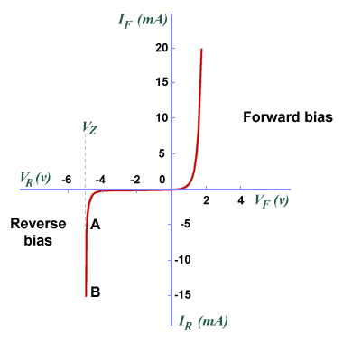
The characteristic voltage and current curve for a Zener diode
You can see from the curve that increasing the reverse voltage has a negligible effect on the reverse current until the breakdown voltage VZ (otherwise known as the Zener voltage) is reached. At this point the current can increase rapidly over a wide range with little or no change in voltage. Notice that the slope of the curve between points A and B on the graph is almost vertical. If the reverse voltage falls below the breakdown voltage once more, the reverse current will again become negligible. In order to limit the reverse current and prevent the Zener diode from overheating, the power rating of the Zener diode should not be exceeded. The maximum reverse current that can be carried can be calculated using the following formula:
| I MAX = | P |
| V |
where:
I MAX = the maximum reverse current
P = the power rating for the diode
V = the Zener voltage
Zener diodes are manufactured with specific Zener voltages ranging from 2.4 V up to 200 V, and a Zener diode with a given Zener voltage can be used in series with an appropriate resistor in a power supply regulator circuit to maintain a steady output voltage, even if the supply voltage itself is prone to fluctuations. The simple voltage regulator circuit shown below uses a single Zener diode (Z) in series with a resistor (R) and a d.c. power supply (in this case, a 12 V dry battery whose voltage is likely to fall over time). The required output voltage is 8 V and the load device will draw a current of 100 mA.
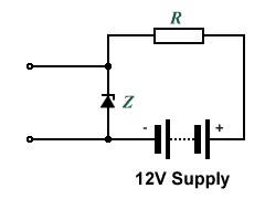
A simple power supply regulator circuit
In this circuit, as long as the supply voltage exceeds the required output voltage (or more accurately the Zener voltage) by a few volts, the voltage across the Zener diode will be stable. Provided we choose a resistor of an appropriate value, the voltage drop across the resistor (VR) should always be the difference between the diode's Zener voltage (VZ) and the supply voltage (VSUPPLY). The closest standard Zener voltage to the required output voltage (8 V) is 8.2 V, which is acceptably close to the target voltage. In addition to the load current, the Zener diode will consume at least another 5 mA so a maximum current value (I MAX) of 110 mA should cover our requirements (a good rule of thumb is to allow between 10% and 20% on top of the load current). We should also select a Zener diode with a suitable power rating to enable it to cope with the maximum current likely to flow through it (I MAX). The maximum power dissipated in the diode can be calculated as:
VZ × IMAX = 8.2 V × 0.110 A = 0.902 W
The lowest standard power rating for a Zener diode that exceeds this value is 1.3 watts, which should be perfectly adequate. As already mentioned, the voltage dropped across the resistor will be the difference between the source voltage and the Zener voltage (12 V - 8.2 V = 3.8 V). Using Ohm's law, we can calculate the required resistance value as follows:
| VR | = | 3.8 V | = 34.545 Ω |
| IMAX | 0.110 A |
The nearest standard resistor value that exceeds 34.545 Ω is 39 Ω. We should also make sure that the power rating of the resistor is up to the job. We can calculate the power dissipated in the resistor as:
VR × IMAX = 3.8 V × 0.110 A = 0.418 W
If we could be reasonably sure that the supply voltage will never exceed 12 V we could probably get away with a 0.5 W rated resistor, although it might be prudent to choose a 1 W or 2 W rated resistor, just to be on the safe side. In fact, it is always worth considering the possibility of an over-voltage situation arising when dealing with relatively unstable power supplies, and allow for it when selecting circuit components.